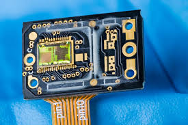
Signals Transmitted on Flexible PCBs
In the past, electronic devices required heavy, bulky machinery to power them, but modern computing technology and portable electronics allow for them to operate on thin, flexible substrate PCBs. These boards are essential for enabling advanced functionality in sleek, compact gadgets like tablets and digital cameras. However, the flexibility of these PCBs comes with its own unique set of challenges. High-speed signals must be transmitted effectively across a plethora of mechanical stresses in order to avoid data corruption and failure. To address these issues, a careful mix of design considerations, simulation, and testing is needed to ensure that flexible circuit boards can meet the high-performance standards required for critical applications such as industrial machinery and aerospace systems.
Signals are transmitted between layers of a circuit board through holes (vias). There are several different types of vias, each with its own specific function. For example, blind and buried vias are designed to transmit signals between two adjacent layer of the board, while through-hole vias connect components on one side of the circuit board to the other. The type of via used in a design depends on the layer structure, signal speed and length, and other factors.
The length of a signal is one of the biggest factors in determining its strength. As the distance a signal travels increases, its strength decreases. This effect is also exacerbated when the signal frequency becomes higher, making it imperative to consider these factors early in the PCB design process.
To combat these problems, designers can implement several different strategies to improve the quality of flexible pcb, including ground plane designs, impedance control, and grid floor plan layout. For instance, using shadowed line or grid-like ground planes on a flexible PCB can ensure that the 0V reference point remains constant, providing shielding over a large frequency range.
How Are Signals Transmitted on Flexible PCBs?
Additionally, routing high-speed signals as differential pairs can improve noise immunity and reduce electromagnetic interference (EMI) between traces. By utilizing a combination of design improvements and rigorous prototyping, designers can achieve robust, high-speed signal transmission on flexible PCBs, meeting the performance standards required for critical applications like aerospace and medical devices.
As the demand for flexible PCBs continues to grow, designers must carefully consider how to maintain signal integrity in these circuit boards. By addressing manufacturing-related concerns, incorporating simulation-driven iterative design, and collaborating with manufacturers to ensure that chosen materials align with both signal integrity requirements and manufacturability constraints, designers can produce high-speed flex circuit boards that comply with industry standards and deliver the performance necessary for cutting-edge applications.
Flexible PCB traces are routed to accommodate bending and flexing without compromising signal integrity. Designers use techniques like serpentine routing, staggered traces, and controlled impedance routing to minimize signal distortion. Maintaining consistent trace widths and spacing is crucial for controlling impedance and reducing signal loss.
The choice of substrate material significantly impacts signal transmission on flexible PCBs. Polyimide is a common choice due to its excellent flexibility, heat resistance, and dielectric properties. Polyester substrates offer cost-effective alternatives but may have lower thermal resistance. Selecting the appropriate substrate material depends on the application’s requirements for flexibility, temperature range, and performance.